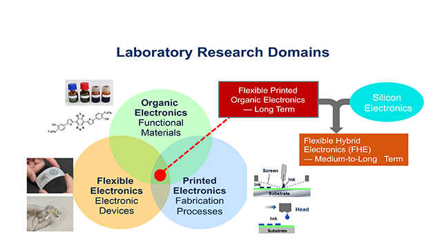
 Laboratory Research Domains
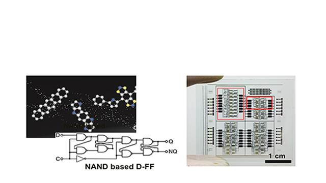 Organic Semiconductor Materials, Devices & Circuits
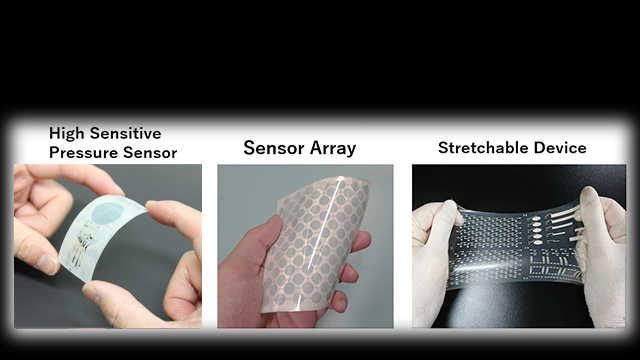 Flexible and Stretchable Printed Physical Sensors
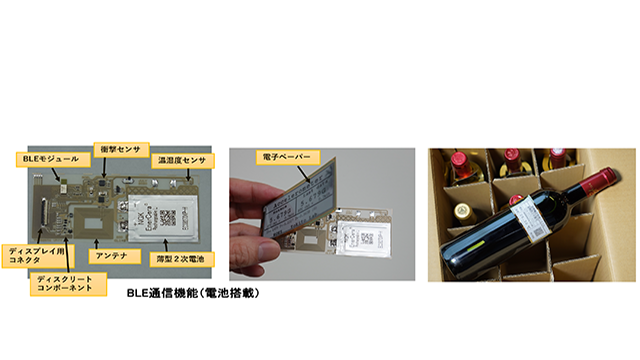 Flexible Hybrid Electronics
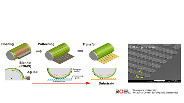 Ultra-Fine Printing Technologies
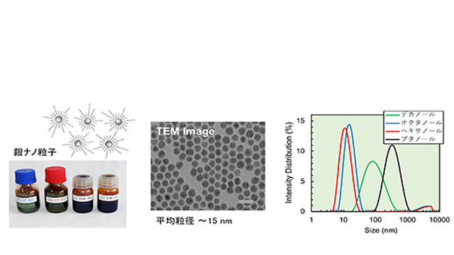 Development of the Metal Nanoparticle Ink
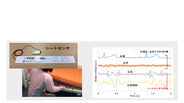 Large-Area Sensor Technologies
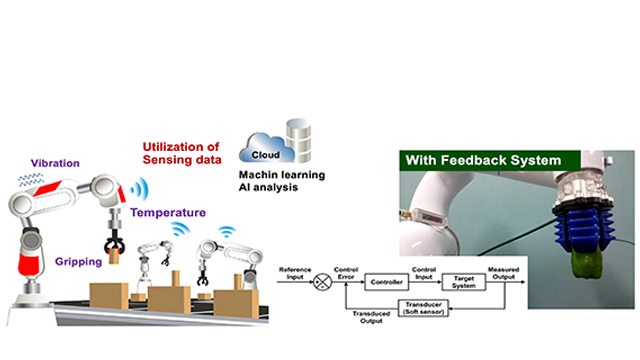 Robotic Sensing Technologies
| New papers | |
 | |
 | |
 | |
 | |


![]()