Current Results
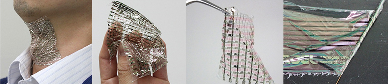
Fully-printed high-performance organic circuitry on ultra-flexible polymer film
Thin, ultra-flexible devices that can be manufactured in a process that covers a large area will be essential to realizing low-cost, wearable electronic applications including foldable displays and medical sensors. Printing technology will be instrumental in fabricating these novel electronic devices and circuits; however,
attaining fully-printed devices on ultra-flexible films in large areas has typically been a challenge.
We reported on fully-printed organic thin-film transistor devices and circuits fabricated on 1-μm-thick parylene-C films with high field-effect mobility (1.0 cm2 V?1 s?1) and fast operating speeds (about 1 ms) at low operating voltages. The devices were extremely light (2 g m?2) and exhibited excellent mechanical stability. The devices remained operational even under 50% compressive strain without significant changes in their performances. These results represent significant progress in the fabrication of fully-printed organic TFT devices and circuits for use in unobtrusive electronic applications such as wearable sensors.
* This work was published in Nature Communications.
Accurate and reproducible detection of proteins in water using an extended-gate type organic transistor biosensor
Significant attention is being devoted to the development of biosensors for use in healthcare applications in order to better address the spread of mental, allergic and lifestyle-related diseases, which has globally become a serious social issue. Proteins such as antibodies and enzymes are abundant in the human body and correlate significantly with such diseases. For example, immunoglobulin G (IgG) exists mainly in blood serum, the concentration of which is closely related to connective tissue diseases such as rheumatoid arthritis.
Field-effect-transistor (FET) biosensors are simple and can be integrated easily into a compact sensor device. In particular, organic FETs (OFETs) can be applied to wearable and disposable biosensors because of their mechanical flexibility and low-cost. For these reasons, we believe that the OFET based biosensors are one of the most promising candidates for portable healthcare devices.
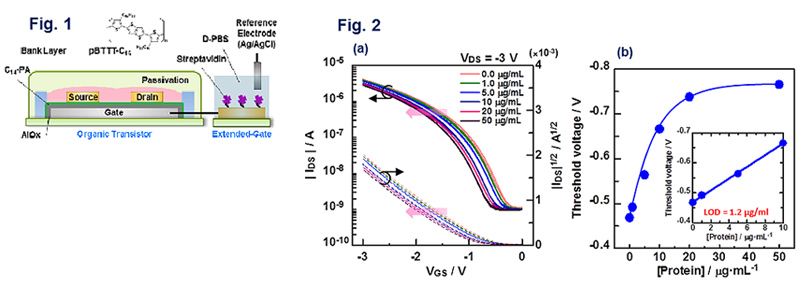
We reported an accurate antibody detection method using a fabricated extended-gate type organic field-effect-transistor (OFET), which can be operated at below three (3) volts. The protein-sensing portion of the designed device is the gate electrode functionalized with streptavidin. Streptavidin possesses high molecular recognition ability for biotin, which specifically allows for the detection of biotinylated proteins. We attempted to detect biotinylated immunoglobulin G (IgG) and observed a shift of threshold voltage of the OFET upon the addition of the antibody in an aqueous solution with a competing BSA interferent. The detection limit for the biotinylated IgG was 8 nM, which indicates the potential utility of the designed device in healthcare applications.
*This work was published in Applied Physics Letters.
Strain-durable printed organic Thin-film transistors for sensor application
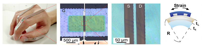
We demonstrated the strain-durable printed organic thin-film transistors (TFTs) with ink-jet printed silver electrodes fabricated from silver nanoparticle inks. The modified silver nanoparticle inks enabled the strong adhesion to the underlying polymer layer, and the fabricated organic TFTs exhibited excellent reproducibility in the bending cycle tests. The strong channel-length-dependence on the strain sensitivity was observed in both p-type and n-type organic TFTs. The organic TFTs with a short-channel exhibited higher sensitivity to the bending strain. These results suggest that the flexible organic TFTs with printed silver electrodes have excellent mechanical durability and are useful for bending and strain sensor applications [1].
The devices were fabricated on 125-μm-thick PEN substrates. The substrates were coated with a planarized polymer layer. The silver nanoparticle ink (JAGLT-01, DIC) was patterned with an inkjet printer (DMP2800, Fujifilm Dimatix) onto the planarization layers. After the printing, the substrates were stored for 30 min in an environmental test chamber (SH-221, espec) in which the temperature was held at 30℃ and relative humidity was held at 95%RH in order to planarize the electrodes [2]. After the drying process, the substrates were heated at 140℃ for 1 hour to sinter the silver nanoparticles. The fabricated silver gate electrodes had an uniform thickness of ~100 nm. A solution of PVP was spin-coated and baked to form 350-nm-thick dielectric layers. The silver electrodes were subsequently inkjet printed. Finally, a 50-nm-thick semiconducting layer made of pentacene or trifluoromethylphenyl groups (FPTBBT) was deposited on the source/drain electrodes.
Both p- and n-type devices on polymer dielectrics exhibited a decrease in saturation on-current upon the application of tensile strain. The transfer characteristics of both p-type and n-type TFTs completely returned to the initial state after the 1.6% tensile strain. The mechanical durability was comparable with previously reported organic TFT devices with evaporated Au electrodes [3], which was attributed to the strong adhesion of the electrodes with the underlying dielectric surfaces. Therefore, these results exhibited the feasibility of applying inkjet-printed electrodes to the flexible electronics.
Furthermore, the electrical characterization was performed for devices with different channel length (L). The strain sensitivity clearly depended on the channel length for both p- and n-type devices. As L shortened, the current became more sensitive to the surface strain. The devices with a high strain sensitivity can be made useful for sensing applications by using a short channel length. In contrast, wider channel length is suitable for decreasing their sensitivity to strain.
[1] K. Fukuda et al., Scientific Reports, 3, 2048 (2013).
[2] K. Fukuda et al., ACS Appl. Mater. Interfaces, 5, 3916 (2013).
[3] T. Sekitani et al., Appl Phys. Lett. 86, 073511 (2005).
*This result was released at MRS Fall 2013
Highly stable bottom-contact organic thin-film transistor with short channel copper source and drain electrodes
We have successfully fabricated a bottom-contact organic thin-film transistor (TFT) with short channel copper (Cu) source and drain (S/D) electrodes. The S/D electrodes with a channel length of 5μm was patterned by photolithography and wet etching process. By treating the Cu S/D electrode with pentafluorobenzenethiol (PFBT), the pentacene TFT showed the field effect mobility of 0.1cm2 /Vs at a Vgs of -20 V, which was comparable to that of similar TFTs with gold (Au) electrodes. We also investigated air stability of the Cu electrode by evaluating the change in the contact resistance in air conditions because significant contact degradation is suspected by the oxidation of Cu electrode.
Aluminum (Al) was deposited on the glass substrate for 50 nm. A 220-nm-thick Teflon was formed by spin-coating on the substrate as gate insulator. Copper was deposited on the Teflon by using thermal evaporation for 50 nm. The Cu layer was patterned by photolithography and wet etching to form S/D electrodes, which have a channel length in the range from 5 μm to 50 μm. We used acid based etchant containing nitric acid, phosphoric acid and acetic acid (Kanto Chemical co., acid etchant) for pattering the Cu layer. After pattering, the Cu S/D electrode was treated with PFBT vapor for 1 min. Finally, pentacene or dinaphthoTTF (DNTTF) [1] was deposited on the substrate as a semiconductor layer. We observed the change in contact resistance in air conditions after initial characteristics was evaluated in nitrogen atmosphere. The contact resistance was estimated by using transmission line method (TLM).
In general, the edge sharpness of the S/D electrode at the channel region is especially important to obtain minimum contact resistance. We have successfully fabricated a fine Cu electrode with no residual on channel region by reducing the ratio of acetic acid. By this improvement, the hysteresis in transfer characteristics was dramatically reduced. The pentacene TFT with Cu S/D electrodes treated with PFBT showed the mobility of 0.1 cm2/Vs at a Vgs of -20 V, which was comparable to that of similar TFT with gold (Au) electrodes. The contact resistance could be reduced from 200 kΩcm to 100 kΩcm at a Vgs of -20 V by using DNTTF because of a shallow ionization potential (4.95 eV) compared to that of pentacene (5.05 eV).
We evaluated the contact degradation of the Cu S/D electrode after exposure to air. In DNTTF TFT without contact treatment, although the contact resistance was slightly increased from 95 to 103 kΩcm at a Vgs of -20 V by exposure to air, it was maintained at almost the same level (105 kΩcm) after storing in air for 50 days. This result indicates that the influence of the oxidation in the Cu electrode is negligible for the transistor performance.
[1] Naraso, et al., J. Am. Chem. Soc. 127, 10142 (2005).
*This result was released at MRS Fall 2013
Channel length dependence of device performances in fully-solution processed flexible organic thin-film transistor array
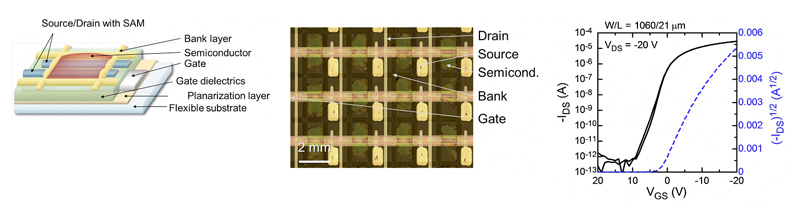
We fabricated fully solution-processed organic thin-film transistors (TFTs) and array with a high yield with as high as 100% and high electrical performance. The treatment layer for source/drain electrodes improves the carrier injection from those electrodes into semiconducting layer, resulting in the low contact resistance. Furthermore, large crystal-domain-sizes of organic semiconductor resulted in the high mobility in the devices with shorter channel length. The highest mobility over 1.2 cm2/Vs was obtained in the devices with a channel length below 20 μm. By combining those fabrication techniques, we demonstrated the organic TFT arrays with average mobility as high as 0.80 cm2/Vs and an ideal threshold voltage of 0 V as well as great performance uniformity.
A 125-μm-thick PEN film was used as a substrate, on which a polymer solution was spin-coated to form a base layer. A silver nanoparticle ink (JAGLT-01, DIC) layer was applied using inkjet printing (Fujifilm Dimatix, DMP2830) and then sintered at 120 oC to form the gate electrode. An insulating material (lisiconR D207, Merck) was then spin-coated to form a 600 nm-thick gate dielectric layer. Silver nanoparticle ink (NPS-JL, Harima Chem.) was then inkjet printed and sintered at 120 oC to form the source-drain electrodes, which were modified using self-assembled monolayer (lisiconR M001, Merck). 200-nm-thick fluoropolymer bank layers were printed by using dispenser equipment (Image Master 350PC, Musashi Engineering). Lastly, an organic semiconducting ink (Merck, lisiconR S1200) was printed using a dispenser equipment and annealed at 100 oC for 1 min.
The fabricated organic TFTs showed specific correlation between the channel length and mobility. the mobility decreases approximately linearly to the channel length in the range from 10 μm to 150 μm. A fitted line has a negative slope and with correlation coefficient R2 of 0.52. A large mobility of 1.2 cm2/Vs was obtained from the device with short channel length of 10 μm. Large crystal domain sizes of semiconducting layer of 30 μm and low contact resistance of 1.8 kΩcm caused this specific channel length dependence of the TFT performance [1].
The fabricated 10 × 10 TFT array on flexible PEN film was operated successfully with yield of 99%. The mobility in the saturation regime was 0.80 ± 0.23 cm2/Vs on average. The threshold voltage was 0.0 ± 1.7 V on average. These performance dispersions are comparable with organic TFTs with evaporated gold source/drain electrodes on glass surfaces [2,3].
[1] D. J. Gundlach et al., Nature Mater. 7, 216-221 (2008).
[2] H. Minemawari et al., Nature 475, 364-367 (2011).
[3] M. Ikawa et al., Nature Commun. 3, 1176 (2012).
This result was released at MRS Fall 2013.
Contact modification using MoOx layer for top-contact organic thin-film transistor
with patterned copper S/D electrode by using photolithography process
We have successfully fabricated a short channel top-contact organic thin-film transistor (TFT) with molybdenum oxide (MoOx) for contact modification and copper (Cu) for source and drain (S/D) electrodes patterned by photolithography process. The top-contact pentacene TFT with Cu S/D electrode showed the mobility of 0.2 cm2/Vs at Vgs of -20 V, which was four times higher than that of bottom-contact pentacene TFT with Cu electrode. Furthermore, the mobility was increased to 0.5 cm2/Vs by introducing MoOx layer between pentacene and Cu electrode to improve the carrier injection property.
Aluminum (Al) was deposited on a glass substrate for 50 nm. A 180-nm-thick crosslinkable poly-4-vinylphenol (PVP) was formed by spin-coating on the substrate as gate insulator. The crosslinkable PVP was prepared by blending melamine, PVP and silane coupling agent. Then, pentacene was deposited on the gate insulator through shadow mask for 50 nm. A Cu layer was deposited by thermal evaporation for 50 nm, and was patterned by photolithography and wet etching. In the case with MoOx layer, molybdenum trioxide was deposited by thermal evaporation before Cu deposition. The bilayer electrode was simultaneously wet-etched by the Cu etchant. Channel lengths were 5 to 20 μm. Finally, the fabricated pentacene TFTs were annealed in dry nitrogen at 120 °C for 2 hours. The electrical characteristics were measured in dry nitrogen by using a semiconductor parameter analyzer.
The pentacene TFT with 5 μm channel showed a high mobility of 0.2 cm2/Vs at Vgs of -20 V, which was four times higher than that of bottom-contact pentacene TFT with Cu electrode. However, the on current was significantly decreased in pentacene TFTs with longer channel. This degradation was observed particularly in longer channel than 10 μm. From these results, the semiconductor channel might be damaged by infiltration of the etchant or water into channel region adjacent to gate insulator through the grain boundary. The grain size of pentacene was 1 to 3 μm, it is therefore considered that the damage was reduced by shortening the channel. Additionally, we have successfully introduced the MoOx layer for improving carrier injection to organic semiconductor. The mobility of the pentacene TFT was increased up to 0.5 cm2/Vs.
*This result was released at MRS Fall 2013