Theme
Organic Semiconductor Materials
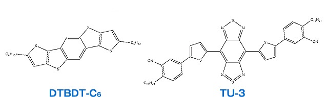
Development of Soluble Organic Semiconductor for Printed Organic Transistors
Background and Objectives
Organic transistor with a channel layer of organic semiconductor (OSC) is expected to employ for flexible displays or wearable devices due to its light and flexible performance, which are difficult to be provided by silicon semiconductor. Printing production technology for the electronic devices is actively studied worldwide in terms of academics and industry because it enables large-area and low-cost mass production utilizing solubility and low-temperature fabrication of OSC. Up to now, however, there are only a few reported examples of OSC integrating high performance with simple and highthroughput printing process. We aim to develop a new soluble OSC solving these technical challenges.
Research Contents
・Development of an original soluble OSC in collaboration with partner lab. and chemical company.
・Evaluation of the synthesized OSC with X-ray, thermal and photometric analysis.
・Development of printing process for organic transistor using vacuum and printing equipment
・Evaluation of electrical characteristics of organic transistor and suitability for printing process.
Organic Integrated Circuit
Background and Objectives
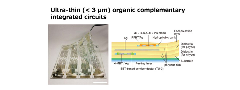
Now that the silicon miniaturization technology is approaching the limit, the semiconductor industry needs a paradigm shift to another direction. Organic semiconductors are expected as a new industrial field because of the unique features such as (1) additive patterning by printing method, (2) high performance at low annealing temperature below 150°C, and (3) the designability of molecules. Compared to solution-processed oxide semiconductors, solution-processed organic semiconductors exhibit higher mobility at annealing temperatures below 250°C. Utilizing these features, we are conducting research and development to realize printed organic integrated circuits on ultrathin plastic films.
Research Contents
We have developed electronic devices on ultrathin plastic films by printing organic semiconductors, ferroelectric polymers and metal nanoparticle inks. The ultrathin (< 3 μm) devices are really flexible, and stretchable when laminated on elastomer sheets. The device characteristics do not change under bending and compression. We will realize patch-type healthcare devices using these technologies.
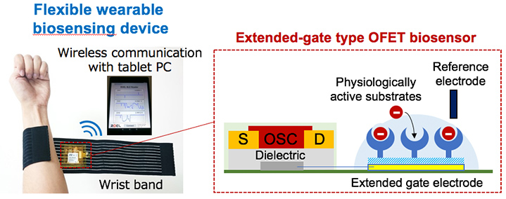
Biosensor
Background and Objectives
Recently, various types of wearable chemical sensors has been developed to realize personal healthcare for a long and healthy life. In this study, we have been developing totally flexible wearable biosensor film composed of an extended-gate type OFET functionalized with bio- and artificial receptors such as enzyme, antibody, and supramolecules.
Research Contents
We have been developed the biosensors for selective detection of physiologically active substrates such as metabolites and immunoglobulins. Now we are challenging to apply this device for noninvasive physiological monitoring by detecting external secretions included in sweat, saliva, or gases.
Ferroelectric Polymer Applications
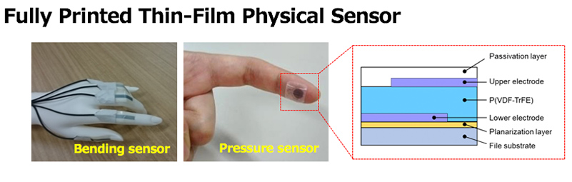
Fully Printed Flexible Physical Sensor with Ferroelectric Polymer, P(VDF-TrFE)
Background and Objectives
Physical sensors based on organic electronics have been attracted in field of the “healthcare”. In this this study, we developed and realized printed pressure sensors and strain sensors with a ferroelectric polymer in order to monitor the human pulse rate and bending angle of the human joints.
Research contents
We have developed flexible printed physical sensors by P(VDF-TrFE) and a conducting polymer, PEDOT:PSS, with a screen printing method. The sensors can monitor the human pulse wave and the human motion only attaching to the skin. Their sensors can realize healthcare/wearable devices by combining printed organic electric circuits on a flexible film substrate.
Flexible Hybrid Electronics
Flexible Hybrid Technology Unifying Printed Organic Circuits and Si-LSIs
Background and Objectives
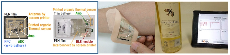
Flexible hybrid sensors have been demonstrated, which unify an organic sensor and conventional silicon LSI for the functions of RF communication and data processing on a flexible substrate using fine printing methods. This lightweight, flexible device can be worn on the human body or attached to objects with irregular or nonplanar surfaces for practical use in the emerging Internet of Things (IoT) society.
Research Contents
Organic thermal sensors, antenna and stacked interconnects are printed on a PEN substrate using the screen printer with functional inks, and small Si-LSI are mounted on the same substrate. This hybrid sensor has approximately a entire thickness of 200μm and integrates the flexibility of organic electronics with the high functionality of Si-LSIs. Sensing the temperature of body skin and commercial goods and transmitting the measured data have been succeeded by hybrid sensors with NFC (near field communication) and BLE (low energy Bluetooth communication). The continuous sensing operation of approximately 6 months is expected to be achieved by the power management with intermittent communication.
Reverse Offset Printing
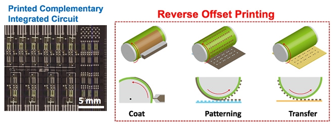
Development of Fine Patterning Technology and Integrated Circuits using Reverse Offset Printing
Background and Objectives
Printed electronics is expected to achieve the low-cost production for large-area electronic devices. Since the reverse offset printing enables precise line and space and flat surface, it is suitable for fabricating the fine electrode and stacking the interconnects of organic transistors. We aim for highdensity and high-performance organic integrated circuits, such as RF tag and amplifier.
Research Contents
・Development of conductive inks for reverse offset printing in collaboration with companies.
・Evaluation of functionality as the interconnects and transistor electrodes.
・Development of printing processe for the integrated circuits having a high usability for printing and surface treatment and a high heat resistance.
・Rapid achievement of integrated circuit by improving the printing process based on the study of high-performance transistors.
・Evaluation of contact resistance by printed four(4)-probe method utilizing the fine patterning.
3D Printed Electronics
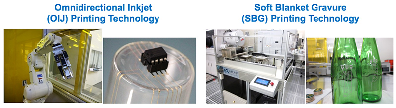
Three Dimensional Printed Electronics Technologies
Background and Objectives
We have developed next generation printing technologies which can print various patterns onto curved or 3D objects surfaces, for patterning technology that was limited to only flat surfaces. We can realize various ideas that change wiring harness to printed wiring, or propose new electric devices.
Research Contents
Omnidirectional Inkjet (OIJ) Printing Technology : OIJ printer is consisted by our original inkjet system put on a tip of articulated robot. It can print patterns on 3D object surfaces like human arm hunging a pen drow picture.
Soft Blanket Gravure (SBG) Printing Technology : SBG printing has a very soft and thick offset roller which called soft blanket and print onto curved surfaces because the soft blanket surfaces change along the surfaces.
Metal Nanoparticle Ink
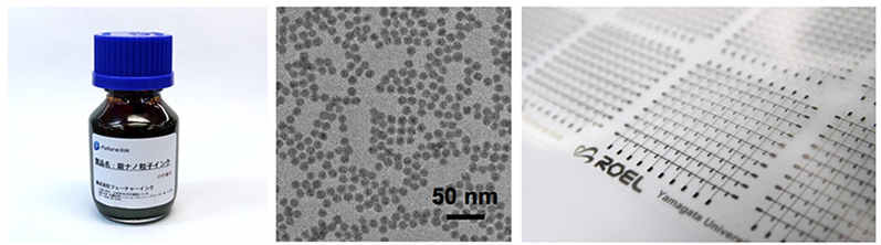
Development of Silver Nanoparticle Ink for High-resolution Printed TFT Curcuits
Background and Objectives
In the printed TFT circuit, it is necessary to form a thin (100 to 200 nm) and a low resistance (10 μΩ ・cm or less) electrode in a fine pattern. We have newly developed a high performance silver nanoparticle ink that can be applied to fine printing system (Reverse off-set printing, Inkjet printing etc). Additionally it is suitable for forming TFT electrode with low resistance at low temperature sintering (150 degree or lower). By controlling the organic surfactant on silver nanoparticles, we have achieved stable dispersion, high printability and excellent electrical performance.
Large Area Printing Technology
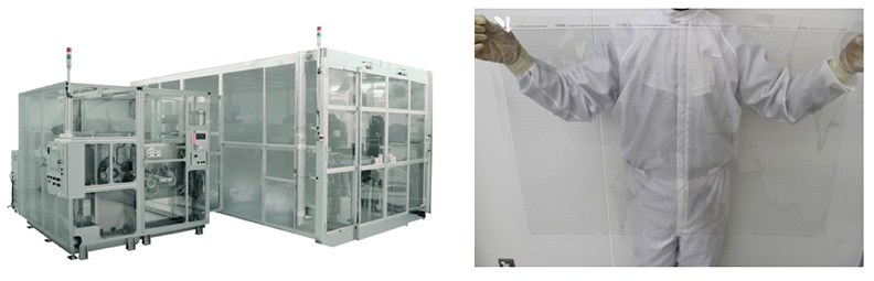
Development of Printing TFT Process using Roll to Roll Inkjet Printing System
Background and Objectives
As the ultimate device manufacturing method using a printing process, there is a roll-to-roll printing in which film is continuously flowed. In the case of forming a TFT circuit directly on a film, it is indispensable that an advanced printing process technology with highly accurate overprinting while correcting with the pattern deformation by contraction of the film.
Research Contents
We are developing the TFT fabrication process on a large area film using a roll-to-roll inkjet printing system with a film width of 900 mm.